The most crucial phase in electronic production is PCB fabrication, which must happen as accurately planned and fabricated down to the minute details. The PCB of a device determines its performance, size, and shape. To meet the design and certification standards, such a complex component that we see inside every electronic device must go through multiple processes. And, to maintain the requirements, each process must be supervised by trained personnel.
Even though the time it takes to complete the steps may vary according to the complexity of the circuit, the number of steps remains the same. The following are critical steps in PCB manufacturing that give new designers the basic PCB manufacturing process.
1. Design
Clients can submit their PCB designs or ask PCB manufacturers to design them, who do designing also. In both cases, clients have to check the circuitry, shape, size, and controlled impedance before starting actual manufacturing. There is software to design, check the PCB circuit, and route, from which designers have to download Gerber files.
Designers must send the Gerber to the manufacturer along with a DFM (Design For Manufacturing) and BOM (Bill Of Material). These files include schematic images of the PCB circuit (all layers), all needed components, the manufacturing process, testing, compliance requirements, and other information regarding the design.
2. Film generation
Each layer's circuit diagram from the Gerber file is reproduced onto a film. For inner layers, a negative film in black ink represents the copper traces of the PCB. It is the inverse for the outer layers, white for traces, and black for etched. Also, the via holes are drilled on these films.
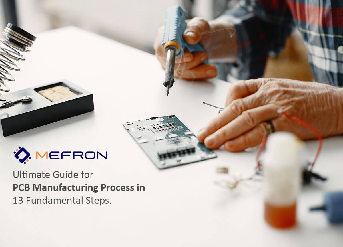
3. Printing
Now the pattern in the film must copy into the copper plates, where the schematic has to print.
Then, each copper plate is laminated with a core, thoroughly cleaned, and treated with a photoresist chemical. The already formed film is then placed over the copper plate and exposed to UV light. Light travels through the film's transparent sections and hardens the photoresist chemical. Later, remove the photoresist with an alkaline solution that eliminates any unhardened photoresist. This process is the printing of the circuit on the copper plate.
4. Etching
Etching is the process of removing unwanted copper from a copper plate, leaving only the copper traces. Unwanted copper is either chemically or mechanically etched away.
5. Lamination
Each layer is inspected and checked whether they are aligned correctly. Also, check the perfection of trace formations. Then each layer is stacked up with prepregs between each copper layer as per the design stack up order. The layers are bonded together by pressing the layers together.
6. Drilling
After the lamination of the layers, it's the turn to drill the vias on the board. Every hole drilled on PCB will follow the requirements of size and type (blinded, through-hole vias, microvias). X-ray locators employed to locate the vias on the board precisely find locations where vias have to drill. The most common drilling techniques are mechanical drilling and laser drilling. Laser drilling is ideal for microvias and blind-via creation because it is precise and fast.
7. Copper plating
Following drilling, vias are copper plated, which means that the wall of the via holes is coated to aid conductivity using the electroplating procedure. Before beginning this process, the vias must clear of debris of drilling. It is now a computer-assisted procedure.
8. Outerlayer process
The processes mentioned above, from printing through copper plating, are repeated for the outer layers.
9. Solder masking
Before solder masking, the board has to clean well. Then an epoxy coating is applied to both sides of the PCB. This process is called solder masking. It can be in any color, like the green, yellow, white, or red-colored layer we see on every PCB board. It shields the board, particularly the traces, from interference and the outside environment (oxidation).
10. Surface finish
For extra solderability of each node that connection point between trace and component, surface finish is added. It also protects the copper from oxidation. ENIG (Electroless Nickel Immersion Gold), ENEPIG (Electroless Nickel Electroless Palladium Immersion Gold), Electrolytic Nickel/Gold - Ni/Au (Hard/Soft Gold), Immersion Silver, White Tin or Immersion Tin are the commonly used surface finishes.
11. Silkscreen
It's the process of labeling each component name on the solder mask with ink. Also, adding logos, symbols, polarity markings, etc.
12. Testing
The PCB is electrically tested to confirm that the traces and vias are connected and functioning as expected, either manually or with a flying probe tester.
13. Assembly
All the components on the BOM are assembled on the PCB using an assembly machine or manually. Then the components are soldered to the traces. Then the PCB is again tested if the designer needs to.
Conclusion
Several phases in the preceding procedures, such as labeling and testing, can be skipped as per the designer's requirements. There are also various ways to complete each phase, determined by the designer's needs, money, and time constraints. Find the ideal PCB manufacturing partner to help you transform your unique concepts into actual PCBs. You may contact us at any time at: sales@mefron.com