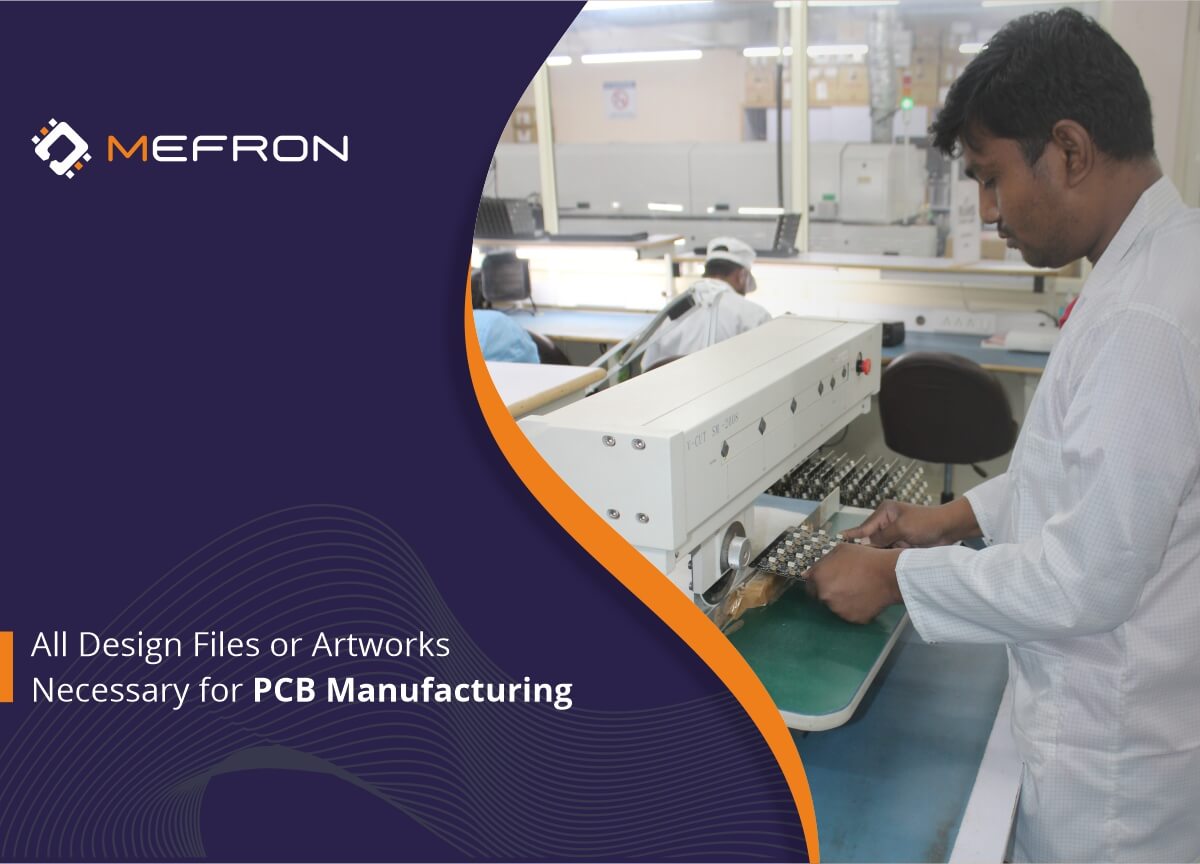
All Design Files or Artworks Necessary for PCB Manufacturing
PCB manufacturing involves complex procedures that are not simple to explain to the manufacturer. There is a set of standard files every designer must forward to the PCB manufacturer to convey the design prospects. These set files, also known as artworks, are suitable for uploading to automatic PCB fabricating machines. So a designer's primary objective is to give detailed files. They can generate these files from all designing platforms like KiCad, Altium, Eagle, Cadence, etc.
On the other side, manufacturers can determine the design's manufacturability by running the artwork on software. Also, some types of files in design files are machine-readable, which helps automate several processes. First of all, designers have to make sure they have produced the following list of files.
Design files required for PCB manufacturing
Each major step in PCB manufacturing requires its design file, and each of those files must designate independently with unique extensions. Design files are the communication link between designers and fabricators. Hence each file must create and arrange following the standards and specifies the design in detail.
The necessary files are:
Gerber
Gerber is a standard ASCII file generated for each layer of a PCB. Each layer requires a separate file distinct from the others, with a different file name. In addition to the files for each layer, designers have to generate Gerber for all fabrication procedures like silkscreen, etching, drilling, etc. This standard file comes in three formats; RS-274D, RS-274X (also known as Excellon), and the latest X2 version. The standard extension used for the Gerber file is .gbr
Common Gerber file names:
TOP - file for the top layer
BOT - file for the bottom layer
SMT/SMB: solder mask top and bottom
SPT/SPB: solder paste top and bottom
SST/SSB: silkscreen top and bottom
AST/ASB: assembly instruction for top and bottom
FAB: contain details regarding stackup, drill, and the class of PCB
Bill Of Material (BOM)
BOM contains the list of all components required for PCB assembly and its footprints. The designer can generate it from the designing software or manually list it on an excel sheet. Fabricators refer to this document to procure components and in assembling. A BOM must contain:
All components
Footprints
Designators
Component specifications and quantity
Part number, etc
Pick and Place File
It is also known as a centroid file, an ASCII file. The file is used during the assembly process to take the correct device and place it at the exact location on the board. Most mainstream CAD tools can automatically generate the Pick and Place file with the design. The file is in a machine-readable format so that the CNC pick and place machines can read it to automate the assembly process. This file contains:
X-Y coordinates of components
Orientation of component
Position of devices (top or bottom)
Specification of each product
Netlist
Netlist contains the list of all the circuit nets in a PCB. It is an ASCII file following the IPC-356 standards. Both the fabricators and designers generate the netlist from the Gerber files. Fabricators compare it with the designer's netlist so that they can confirm the routing procedure. The list contains the trace width, length, and all the specifications of routes.
Drill Diles
A drill file contains detailed information on the drill position, size, type, and total number of drills. While the drilling process, fabricators use these files to determine the drill hole position. The drill file is checked while preparing each layer to drill through-hole, blind, or buried vias. The number of drill files depends on the complexity of the design and the number of drills required. Besides, separate files must create for plated and non-plated holes. The file extension for plated holes is .drl and np.drl for non plated drills.
FAP Drawings
FAP drawing refers to an overview of PCB schematic design, stackup drawing, and dimensions. Designers may add all relevant data on the FAP drawing in the 'Notes' section. Designers may also use this graphic to incorporate their brand logo. The FAP drawing is exported in PDF format.
Conclusion
Designers must make sure design files have plenty of details that ensure an undoubtful fabrication process. Anyway, PCB manufacturers will verify the files with the help of software and technology experts. The artwork files demonstrate the PCB being manufactured in a simple compiled way, reducing the need for verbal descriptions. Manufacturers respond to designers with a prototype. The manufacturing time period may vary according to the complexity and PCB class.